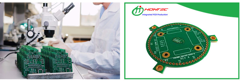
Quick Details of VIA in PAD PCB
Place of Origin: Guangdong, China
Brand Name: Communication network PCB Model Number: Rigid-PCB
Base Material: ShengYi
Copper Thickness: 1oz Board Thickness: 2mm
Min. Hole Size: 0.2mm Min. Line Width: 3.94mil Min. Line Spacing: 3.94mil
Surface Finishing: ENIG
Max Layer: 12L PCB Standard: IPC-A-600
Solder Mask:Green
Legend:White
Product quotation: Within 2 Hours
Service: 24Hours technical services Sample delivery: Within 10 days

 You are here :